NAND FLASH Packaging
As the demand for miniaturized products increases and wearable devices become more widespread, engineers are increasingly focused on the miniaturization of chips, which brings us to chip packaging technology. This time, we will focus on introducing the packaging of NAND flash.
Common chip packaging types include DIP, QFP, PFP, PGA, BGA, TSOP, and COB. Here, we will mainly introduce the three packaging types commonly used for NAND FLASH: TSOP, BGA, and COB.

1. TSOP Packaging
TSOP stands for "Thin Small Outline Package." In TSOP packaging, pins are arranged around the chip, which is then attached to the surface of a PCB using Surface Mount Technology (SMT). The assembly height is less than 1.27mm. Specifically, for FLASH-type chips, the process involves fixing the FLASH wafer onto a steel frame, connecting points on the wafer to the frame's pins through wire bonding, and then encapsulating the surface.
Currently, the most advanced technology can encapsulate four wafers within a single TSOP FLASH package. TSOP packages tend to be relatively thick. The key features of TSOP packaging include minimal voltage fluctuations during significant current changes, making it suitable for high-frequency applications. It's also user-friendly (e.g., easy for manual placement or rework) and highly reliable. Additionally, TSOP packaging offers a high yield rate, although it is relatively more expensive than COB. This has led to its widespread adoption.
2. COB Packaging
COB, or "Chip on Board," is a type of bare die mounting technology. In COB packaging, semiconductor chips are directly mounted onto a printed circuit board (PCB), and the chip is connected to the PCB through bonding. The primary reason for using COB packaging in the NAND FLASH industry is cost efficiency. Engineers first design the peripheral circuitry, then apply red adhesive to the PCB and position the wafer in the specified orientation.
The wafer is then bonded using a bonding machine. After ensuring the electrical performance of the bond is good, the wafer surface and part of the PCB are covered with resin to secure them. COB is the simplest form of bare die mounting technology, but its packaging density is much lower than that of TSOP and BGA technologies.
3. BGA Packaging

BGA, or Ball Grid Array, is a type of surface mount packaging that uses spherical solder balls arranged in a grid pattern on the backside of the printed circuit board (PCB) instead of traditional pins. The NAND flash chip is mounted on the front side of the PCB, and then the package is sealed with either molded resin or an encapsulation method. The package size can be made smaller than that of QFP (Quad Flat Package).
Key Features of BGA:
1. Increased I/O Pin Count: While the number of I/O pins increases, the distance between the pins is much greater compared to QFP packaging, which improves the yield rate.
2. Enhanced Electrical and Thermal Performance: Despite the increased power consumption of BGA, the use of controlled collapse chip connection (C4) soldering can improve electrical and thermal performance.
3. Lower Signal Transmission Delay: BGA packaging results in minimal signal transmission delay, which significantly increases the operating frequency.
4. Reliable Assembly: BGA allows for co-planar soldering, which greatly enhances reliability.
In the context of NAND FLASH, BGA packaging offers the following advantages:
1. Suitable for Large Wafer Sizes: It can accommodate the packaging of larger wafers.
2. Space Efficiency: BGA packaging reduces the footprint of the NAND flash chip, making it ideal for products with stringent size requirements, such as wearable devices, where product dimensions are critical.
3. Primarily Used for Original Chips: BGA packaging is mostly used for original chips, with black market chips being less frequently packaged in BGA.
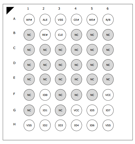
From the above, it is clear that BGA packaging is well-suited for miniaturization needs. For instance, the Korean company ATO Solution offers 1Gb NAND flash in a BGA package with a minimum size of 6.5 x 8 mm (48-ball), compared to the standard 1Gb NAND flash size of 9 x 9 mm (48-ball). This makes BGA an excellent choice for customers with strict space requirements in their products.

